- 您现在的位置:买卖IC网 > Sheet目录316 > BU9829GUL-WE2 (Rohm Semiconductor)IC EEPROM 16KBIT SPI 9VCSP
�� �
�
�BU9829GUL-W� (16Kbit)�
�Datasheet�
�●� Functional� description�
�○� Status� Register�
�The� device� has� status� register.�
�Status� register� consists� of� 8bits� and� is� shown� following� parameters.�
�2� bits� (BP0� and� BP1)� are� set� by� “Write� Status� Register”� commands,� which� are� non-volatile.�
�Specification� of� endurance� and� data� retention� are� as� well� as� memory� array.� WEN� bit� is� set� by� “Write� Enable”� and� “Write�
�Disable”� commands.� After� power� become� on,� the� device� is� disable� mode.� R� /� B� bit� is� a� read-only� and� status� bit.�
�The� device� is� clocked� out� value� of� the� status� register� by� “Read� Status� Register”� command� input.�
�Bit7�
�0�
�Bit6�
�0�
�Bit5�
�0�
�Bit4�
�0�
�Bit3�
�BP1�
�Bit2�
�BP0�
�Bit1�
�WEN�
�Bit0�
�R� /� B�
�Bit�
�BP0/BP1�
�WEN�
�Definition�
�Block� write� protection� for� memory� array�
�(EEPROM)�
�Write� enable/disable� status� bit�
�WEN=0� :� write� disable�
�WEN=1� :� write� enable�
�BP1�
�0�
�0�
�1�
�1�
�BP0�
�0�
�1�
�0�
�1�
�Block� Write� Protection�
�NONE�
�600h-7FFh�
�400h-7FFh�
�000h-7FFh�
�READY/BUSY� status� bit�
�R� /� B�
�R� /� B� =0� :� READY�
�R� /� B� =1� :� BUSY�
�●� Instruction� code�
�Instruction�
�Operation�
�Op.Code�
�Address�
�WREN�
�WRDI�
�READ�
�WRITE�
�RDSR�
�WRSR�
�VSET_READ�
�VSET_WRITE�
�Write� enable�
�Write� disable�
�Read� data� from� memory� array�
�Write� data� to� memory� array�
�Read� status� register�
�Write� status� register�
�Read� VSET� data�
�Write� VSET� data�
�0000�
�0000�
�0000�
�0000�
�0000�
�0000�
�0000�
�0000�
�0110�
�0100�
�0011�
�0010�
�0101�
�0001�
�0011�
�0010�
�-�
�-�
�A10� to� A0�
�A10� to� A0�
�-�
�-�
�800h�
�800h�
�●� Timing� chart�
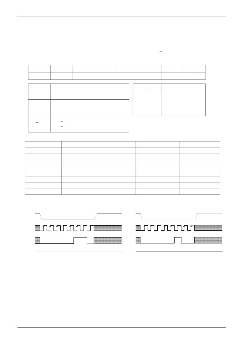
�1.� WRITE� ENABLE�
�CSB�
�2.� WRITE� DISABLE�
�CSB�
�SCK�
�SI�
�0�
�0�
�0�
�1�
�0�
�2�
�0�
�3�
�0�
�4�
�1�
�5�
�1�
�6�
�0�
�7�
�SCK�
�SI�
�0�
�0�
�0�
�1�
�0�
�2�
�0�
�3�
�0�
�4�
�1�
�5�
�0�
�6�
�0�
�7�
�SO�
�Hi-Z�
�Figure� 31.� WRITE� ENABLE� CYCLE� TIMING�
�SO�
�Hi-Z�
�Figure� 32.� WRITE� DISABLE� CYCLE� TIMING�
�○� The� device� has� both� of� the� enable� and� disable� mode.� After� “Write� Enable”� is� executed,� the� device� becomes� in� the� enable�
�mode.� After� “Write� Disable”� is� executed,� the� device� becomes� in� the� disable� mode.� After� CSB� goes� low,� each� of� Op.code�
�is� recognized� at� the� rising� edge� of� 7th� clock.� Each� of� instructions� is� effective� inputting� seven� or� more� SCK� clocks.� This�
�“Write� Enable”� instruction� must� be� proceeded� before� the� any� write� commands.� The� device� ignores� inputting� the� any� write�
�commands� in� the� disable� mode.� Once� the� any� write� commands� is� executed� in� the� enable� mode,� the� device� becomes� the�
�disable� mode.� After� the� power� become� on,� the� device� is� in� the� disable� mode.�
�www.rohm.com�
�?� 2012� ROHM� Co.,� Ltd.� All� rights� reserved.�
�TSZ22111� ?� 15� ?� 001�
�13/23�
�TSZ02201-0R2R0G100400-1-2�
�28.AUG.2012� Rev.001�
�发布紧急采购,3分钟左右您将得到回复。
相关PDF资料
BU9832GUL-WE2
IC EEPROM 8KBIT SPI VCSP50L2 TR
BU9833GUL-WE2
IC EEPROM 2KBIT 100KHZ VCSP50L1
BU9844GUL-WE2
IC EEPROM 16KBIT 2WIRE VCSP50L1
BU9847GUL-WE2
IC EEPROM 4KBIT 2WIRE VCSP50L1
BU9880GUL-WE2
IC EEPROM 64KBIT 2WIRE VCSP50L1
BU9882FV-WE2
IC EEPROM 2KBIT 400KHZ 14SSOP
BU9883FV-WE2
IC EEPROM 6KBIT 400KHZ SSOP16
BU9889GUL-WE2
IC EEPROM 8KBIT 2WIRE VCSP50L1
相关代理商/技术参数
BU9831
制造商:ROHM 制造商全称:Rohm 功能描述:Non-volatile electronic potentiometer
BU9831F
制造商:ROHM 制造商全称:Rohm 功能描述:Non-volatile electronic potentiometer
BU9832GUL-W
制造商:ROHM 制造商全称:Rohm 功能描述:WL-CSP EEPROM family SPI BUS
BU9832GUL-W_10
制造商:ROHM 制造商全称:Rohm 功能描述:WL-CSP EEPROM family SPI BUS
BU9832GUL-WE2
功能描述:电可擦除可编程只读存储器 电可擦除可编程只读存储器 Serial-SPI 8Kb
RoHS:否 制造商:Atmel 存储容量:2 Kbit 组织:256 B x 8 数据保留:100 yr 最大时钟频率:1000 KHz 最大工作电流:6 uA 工作电源电压:1.7 V to 5.5 V 最大工作温度:+ 85 C 安装风格:SMD/SMT 封装 / 箱体:SOIC-8
BU9833GUL-W
制造商:ROHM 制造商全称:Rohm 功能描述:Silicon Monolithic Integrated Circuit
BU9833GUL-W_10
制造商:ROHM 制造商全称:Rohm 功能描述:WL-CSP EEPROM family I2C BUS
BU9833GUL-WE2
功能描述:IC EEPROM 2KBIT 100KHZ VCSP50L1 RoHS:是 类别:集成电路 (IC) >> 存储器 系列:- 标准包装:2,000 系列:- 格式 - 存储器:RAM 存储器类型:SRAM - 异步 存储容量:256K (32K x 8) 速度:15ns 接口:并联 电源电压:3 V ~ 3.6 V 工作温度:-40°C ~ 85°C 封装/外壳:28-TSSOP(0.465",11.8mm 宽) 供应商设备封装:28-TSOP 包装:带卷 (TR) 其它名称:71V256SA15PZGI8